Techinical Data- page 2
In addition to the control signals there are also the following signals:
BA1, BA2 - bank address bits, there two bits determine which of the 4 possebile banks in the SDRAM the command is directed to.
the 10th address bit A10 is also used to expand commands for commands in which it is not needed
(collum addresses are only 11 bits and so can be represented using A0-A9 and A11, and some of the commands do not require an address)
The following commands can be sent using the control signals :
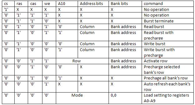
ACTIVATE : this command gives the SDRAM a bank address [ 2 bits deciding which of the up to 4 banks the sdram can possess is addressed now.] and a row address(the row address also requires the A10 bit so it has no special use for the command)
And the contents of row of the bank is read into the array of column content sense amplifiers of the bank, the data is now available for access.
as a side effect the activation also refreshes the charge on that row's capacitors helping to prevent loss of data.
The activation is not immediate, and so during the row to column time (known as t,rcd) Read and write operations cannot be performed on the bank, although the other banks can still be accessed, enforcing this time limitation on incoming requests is handled through the SDRAM controller.
READ/WRITE : once a bank has been activated, requests for the current row can be handled.
A read request would cause the SDRAM to send the Data in the row to the DQ lines after the cas latency time(2 or 3 clock cycles )
A write request causes the data in the DQ lines to be written to the bank's row.
Precharging: once a row has been activated , it must be 'closed' before a new row can be activated, this is because the sense amplifiers in the bank must be returned to idle state, so the next row's content can be read.
there are two ways to command the SDRAM to precharge.
The first is through the precharge command that according to the value of A10 Either charges the chosen bank, or all banks.
The second is by appending a read/write request with a precharge request, done by sending a read/write command with A10 on High.
Auto refresh: the auto refresh command refreshes a row in each bank, the banks must be precharged for the refreshing to be possible , the SDRAM has an internal counter that causes it to change the selected row every refresh interval(t,ref) and so the controller can prevent data loss due to capacitor leakage by sending an Auto refresh command every refresh interval so the rows are refreshed as soon as possebile.
Mode loading: the SDRAM has 10 bits M0-M9 that define the mode it is working in
When the Mode loading command is given each of the bits M0-M9 receives the value of the address bit of the same number (A0->M0.)
The bits control:
M9- decides if the SDRAM would be in burst or no burst write(read is always in burst mode)
M8 and M7 - reserved and must be defined as '0' when the Mode is loaded
M6 ,M5 and M4 Define the CAS latency, typically It would be either 2(0,1,0) or 3(0,1,1)
M3- defines if the SDRAM uses sequential burst or interleaved burst
M2,M1 and M0 Define the size of read bursts and write bursts if M9 is '1'
The size can be 1,2,4 or 8 words.
As you can see from the technical analysis of the SDRAM, it has no direct contact with its host, instead all requests are handled by the controler which sends the appropriate control signals to the SDRAM.
in order to fully understand how the sdram works, it is thus necessary to explain how the controller works.
To that purpose the tutorial includes both a written explanation and an interactive simulation to help understand the controller.